


Test It Until it Fails
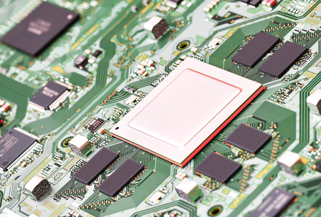
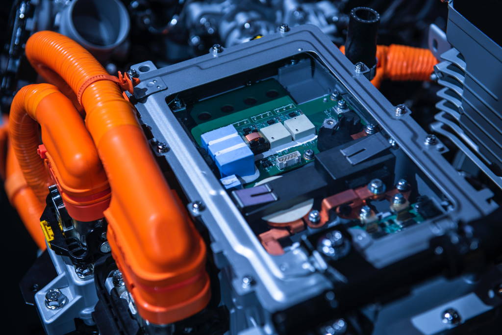
The increasing desire for “High Reliability” Printed Circuit Boards (PCBs) that are the backbone for technology that has driven us to try to better understand the factors that affect the long-term interconnection and isolation reliability of the electrical circuits that comprise a PCB. As the via structures that interconnect components and layers in a PCB are typically the weak point in a conductive circuit, testing requirements have rapidly evolved attempting to assess the Process Survivability, Robustness and Reliability of via structures.
Process Survivability, Reliability Testing and Robustness Testing are terms that tend to be confused with each other and lumped into “Reliability Testing”. I would like to clarify these terms and show how they fit together into the PCB world so that it is clearly understood what it means when each is used.
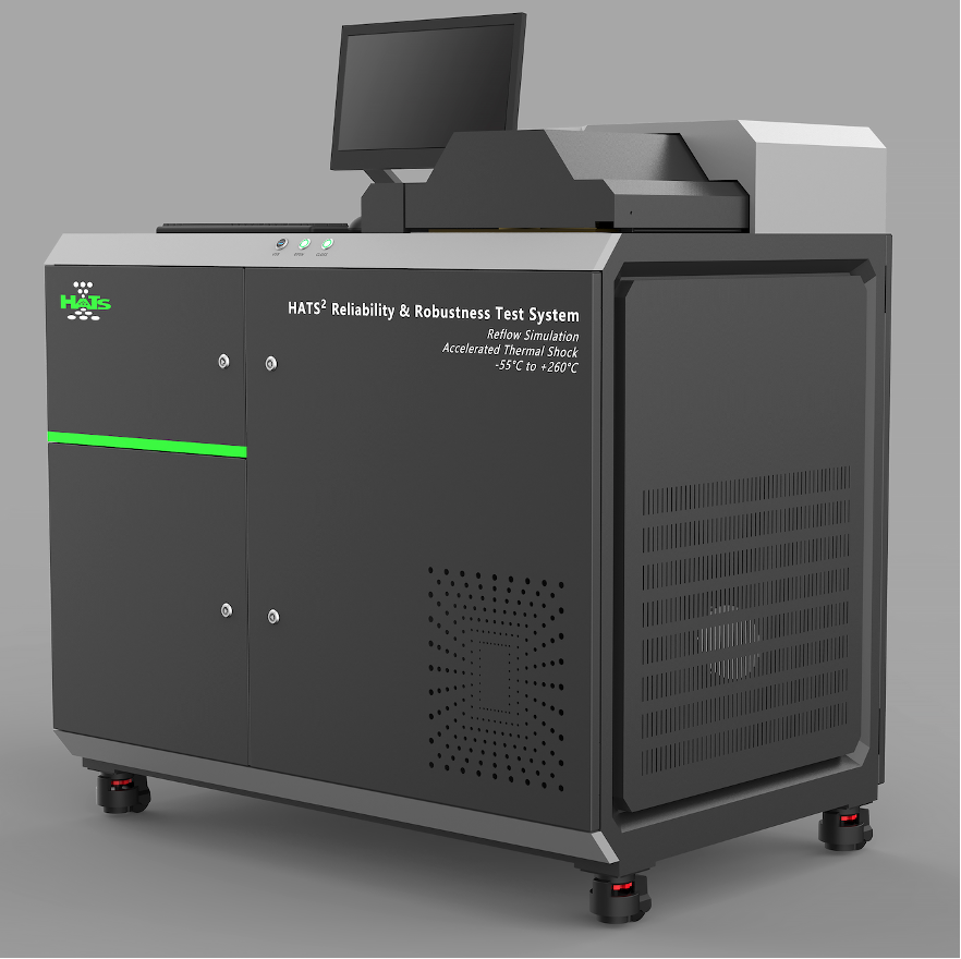
Process Survivability testing is the simulation of the environmental stresses experienced by the PCB during the component attachment process including any repair or rework that might be allowed prior to the product going into use in the field. This means that a representative test sample must be subjected to multiple exposures of the test temperatures utilized for component attachment and rework/repair processes. As this represents what could happen to a PCB during component attachment, process survivability simulation should be performed prior to any reliability or robustness testing. The IPC recently published IPC-TM-650 2.6.27B that defines assembly reflow process survivability testing for via structures. This test method defines the testing of via resistance during the simulation of a convection reflow oven environment. The results of this testing will allow understanding of whether the vias are capable of surviving the multiple reflow/rework/repair processes that are allowed during component attachment. An extension of this test is also sometimes used as a robustness test where reflow simulation cycles are repeated until via structure failure.
Reliability Testing is the process of creating an environment for test samples that significantly accelerates the factors that influence a PCBs performance during its expected life. The results from testing in this environmental acceleration can be evaluated using mathematical models (Weibull, etc.) in order to predict the expected life of the product in the field. Reliability testing attempts to maximize acceleration factors actually seen by the product during its life and eliminate acceleration factors that cannot be directly correlated to real life use.
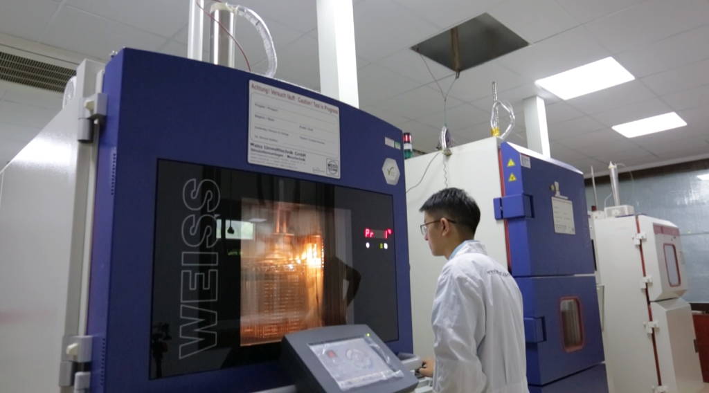
In order to assess the long-term reliability of via structures, thermal shock/cycling is performed on test samples in accordance with IPC-TM-650 method 2.6.7.2 between -55°C to (Tg-10)°C. Keeping the upper temperature that the samples are exposed to 10°C below the Tg ensures that the expansion rate of the material is consistent with what is expected during the life of the PCB. The resistance of single vias or daisy-chains of vias is monitored during thermal shock/cycling and resistance increases over time are indicative of cracking or separation in the via structure(s).
When assessing the long-term reliability of a PCBs insulation system, testing for conductive anodic filaments (CAF) in accordance with IPC-TM-650 method 2.6.25 is normally performed. This testing exposes parallel via structures to 85°C and 85%RH environment while placing a 100VDC potential across them. Electric vehicle electronic systems often run at voltages well above 100V and variations of CAF testing up to 4000VDC have been done at at my facilities. There is no standard for CAF testing at voltages above 100VDC and custom fixtures, cabling and safety systems must be deployed to properly perform high-voltage CAF testing.
Robustness testing is essentially Reliability and/or Survivability Testing Plus. The Plus includes environmental or electrical acceleration factors that cannot be directly correlated to the factors that influence a PCBs long term performance during its expected life. This creates stresses that accelerate failures faster than possible with reliability testing. Robustness testing is used in situations where obtaining faster results is more important than directly understanding life expectancy in the field. These types of tests typically expose PCB test samples to temperatures above the material’s glass transition temperature (Tg) or pressures higher than 1 atmosphere. These conditions create stresses and acceleration factors that are not seen during a product’s normal life. These types of tests are useful when comparing materials, processes or products to each other. After exposure to the extraordinary test conditions of robustness testing, observations point to the “better” one, but that may or may not mean that the better one will outperform “worse” ones in a product’s real-life use environment.
For Via Structures, robustness testing usually means Thermal Shock/Cycling between 25°C and 190-260°C, well above the Tg of the PCBs material. Z-Axis expansion rates of the PCBs substrate material above Tg are 4-10 times what is experienced below Tg and causes extreme stress to the via structures that does not occur during the product’s life. These additional acceleration factors speed the via structures time to demise but creates difficulty when trying to correlate the results to real world operating conditions.
The factors that affect the performance of plated via structures in the PCB are multiple and interact in a way that makes it challenging to identify the interactions that affect the via. Design, layer count, thickness, stackup, material selection, lamination, surface preparation, via formation technique (a subsystem in itself), surface finish and the interaction between all of these affect reliability. This makes modeling and predictive assessment of reliability virtually impossible.